
Abstract : Based on SoPC technology, a signal generator specially designed to stimulate the ultrasonic guided wave of pipeline is designed. The design method of the dedicated DDSIP core for guided wave is elaborated. The generator uses the MicroBlaze soft core processor as the control core, and the single-chip FPGA is supplemented with the necessary small amount of peripheral hardware circuits, which is easy to expand and upgrade. The experimental results show that the output signal has high accuracy, low noise, good stability, and continuously adjustable frequency, which can be easily applied to the detection of ultrasonic guided waves in pipelines.
In the inspection of pipeline defects, the ultrasonic guided wave detection technology has the advantages of smaller attenuation along the propagation path and far propagation distance than the traditional non-destructive testing methods, and the characteristics of the vibration of the particles caused by the particles throughout the interior and surface of the components, thus exhibiting greater advantages[1]. ]. Ultrasonic guided wave has multi-modality and dispersion characteristics in the process of propagation. If the excitation source is not properly selected, the guided wave will be seriously dispersive, which will make the echo signal extremely complex and unfavorable for defect analysis. According to the characteristic curve of guided wave dispersion, it can be seen that in the range of 50 kHz to 500 kHz, the L(0,2) modal ultrasonic guided wave has the fastest and most stable propagation speed, and almost no frequency dispersion occurs. The Hanning window is used to modulate the single-tone signal of a certain number of cycles in this frequency band to form a narrow-band pulse as an excitation source to excite the ultrasonic guided wave dominated by the L(0,2) mode, which can minimize the dispersion. Adverse effects [2].
A variety of ultrasonic guided wave excitation signal generator designs have emerged. One is to use a multifunction function generator such as the HP33120A[3]. Due to the limited storage length of the HP33120A, interference occurs between pulses during long-distance detection, and the highest modulation frequency is not high [4]. The second is the use of single-chip control DDS chip design, high precision, but the customization is weak, and generally requires more than two DDS chips, the cost is expensive. Another method is to use a high-speed MCU to control the D/A converter chip to output the signal directly, which is convenient and easy to implement. However, the accuracy is low, the excitation frequency is limited by the MCU frequency, and it is difficult to continuously adjust. In order to solve the deficiencies of the above design scheme, this design is based on Xilinx's FPGA (Field Programmable Gate Array), using the MicroBlaze soft core processor as the control core, and using the Direct Digital Frequency Synthesizer (DDS) technology to generate a new generation. An Implementation Method of SoPC (System on Programmable Chip) for L (0,2) Modal Ultrasonic Guided Wave Excitation Source. The obtained excitation source has high precision. The number of single-tone sinusoidal waves under the Hanning window modulation is adjustable, and the frequency is continuously adjustable.
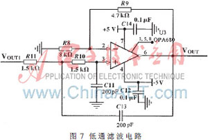
1 Overall System Design The system uses the Xilinx Spartan3E-Starter development board as the hardware platform. This development platform is rich in peripheral resources, and system design can be achieved by adding a small amount of peripheral devices. Spartan3E series FPGA is the most cost-effective FPGA chip of Xilinx, which can better meet the high integration and low cost of products [5]. Its internal MicroBlaze soft processor uses a powerful 32-bit pipelined RISC architecture that contains 32 32-bit general-purpose registers, two 32-bit special registers, and a 3/5-stage pipeline. Clock frequency up to 150MHz. Based on IBM CoreConnect technology, it provides a wealth of interface resources. The PLB (Processor Local Bus) bus provides access to the on-chip peripherals, external memory, and algorithmic blocks written based on the hardware description language. Together with other peripheral IP cores, the embedded SoPC development is completed. The SoPC implementation structure of the ultrasonic guided wave excitation source is shown in FIG. 1 .
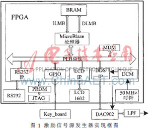 FPGA implements all digital circuit parts. The MicroBlaze soft core processor is the control core of the system. The LMB (local memory bus) accesses the program memory space BRAM, and the PLB bus mounts the required IP core. An example GPIO interface is connected to the keyboard and is responsible for setting the frequency of the stimulus signal. LCD1602 is used for current frequency value display. The independently programmed DDSIP is the core of the system waveform generation and directly generates the excitation source waveform. MDM is the debugging module of the system. RS232 is used to communicate with the PC or program debugging. Using the digital clock of the Xilinx Embedded Development Kit EDK to manage the DCM (Digital Clock Manager) IP core, divide the 50MHz input clock, and provide stable 5MHz and 50MHz clock signals for the DDS module and the external high-speed digital-to-analog converter chip DAC902, respectively. The program is downloaded to the BRAM inside the FPGA through JTAG, or stored in the off-chip PROM. The digital signal generated by the FPGA is converted into an analog signal through the DAC902. After low-pass filter denoising, a high-quality ultrasonic guided wave excitation signal source can be obtained.
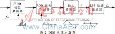
2 ultrasonic guided wave DDSIP nuclear design 2.1 DDS algorithm principle DDS is based on the sampling theorem, through the lookup table method to generate waveforms. Usually sine wave, cosine wave, triangle wave or square wave. The complete DDS structure diagram is shown in Figure 2. Driven by the reference clock, the Nbit phase accumulator accumulates the frequency control word K, and the resulting phase code addresses the waveform memory so that it outputs the corresponding waveform amplitude value. This value is given to the DAC and low-pass filter LPF to achieve the conversion of the quantization amplitude to a smooth signal. When the phase accumulation value is greater than 2N, the phase accumulator generates an overflow and the overflow frequency is the output frequency of the DDS. The output signal frequency fout can be expressed as:
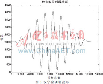
According to the principle of DDS, the number N of phase accumulators determines the accuracy of the DDS. The larger the value of N, the finer the frequency interval of the DDS is. However, as the value of N increases, the required ROM capacity will also increase exponentially. In fact, in the general system, the number of bits of the D/A converter m is fixed. Usually, the number of output bits of the accumulator is set to be N=m+2, which satisfies the requirement [6]. In the design, the DAC902 is 12 bits, the accumulator is 14 bits, and the maximum amplitude of the modulation pulse is 212, which is 4096. With Matlab, a narrow-band pulse waveform is generated that is modulated by a Hanning window for 10 cycles of a sine wave, as shown in FIG. 3 .
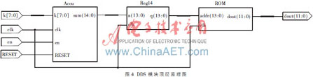
This design is based on DDS technology and uses VerilogHDL hardware description language to design DDS modules that directly generate guided wave excitation waveforms. The top-level principle is shown in Figure 4.
The 50kHz to 500kHz frequency of the L(0,2) modal ultrasonic guided wave refers to the frequency of the single audio signal (as shown in Fig. 3, 10 cycles, setting the tone frequency to f0) instead of the DDS output frequency fout. From Tout = 10T0, fout = f0/10. So the DDS output fout should be 5kHz ~ 50kHz. The main clock of the system is 50MHz. When the DDS output maximum frequency is 50kHz, in order to achieve a 0.3kHz (single audio 3kHz) step value, 10 cycles of narrowband pulse sampling points is not less than 100 points, in order to reduce the distortion, the clock frequency must be greater than 4.9MHz. Divide the system master clock by 10 to get 5MHz DDS clock frequency. Frequency control words take 8bit to meet the requirements.
The Accumulator module Accu accumulates the frequency control word K and sends the resulting lower 14 bits sum[13:0] to the next Reg register as a ROM address. Accu's highest bit sum[14] is a judgment bit. In the accumulation process, when the phase sum[14] is 1, the accumulator is cleared to complete one pulse emission. Then through a counter to achieve delay function, so that the excitation pulse emitted once every 1ms.
The ROM module is directly customized with ROM IP core in ISE. If more than one ROM is added to the system, and each cycle is loaded with modulation pulses of different cycles, the period of the excitation source can be adjusted. With Matlab, the narrowband pulse of Figure 3 is quantized to a 12-bit fixed-point waveform value to form a .coe file and loaded into ROM.
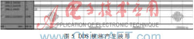
When the frequency control word K is set to 23, the output frequency fout is equal to 7 kHz and the corresponding single audio signal is 70 kHz. Modelsim simulation waveform shown in Figure 5.
3 System Hardware Implementation 3.1 Peripheral IP Core Mounting Using the EDK XPS, the MicroBlaze hardware platform was created. Quickly add configuration via BaseSystemBuilderWizard, such as RS232, GPIO, BRAM, etc. For self-authoring DDS modules, use the Create/ImportPeripheral tool to properly modify the two automatically generated files of userlogic and IPIF. You can attach your own logic module to the PLB bus, without too much concern for custom IP and PLB bus protocol and Interface logic. Add the own DCM clock management module in XPS to provide accurate and stable clock input for DDSIP and DAC. Finally, all peripherals are assigned addresses and port connections are established.

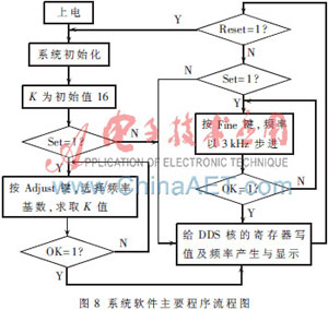
4 The software design software is partially written in the SDK through C language, including initialization, GPIO keyboard value reading, LCD display, DDS frequency word input and adjustment. Due to the guided wave frequency of 50kHz to 500kHz, the span is large. In order to facilitate the actual detection, the frequency coarse adjustment and the fine adjustment function are designed. The system keyboard includes Set key, Adjust key, Fine key, OK key, and Reset key. After power-on, the frequency control word K is the initial value 16. The system generates a 50kHz default frequency excitation signal. Each time you press the coarse adjustment button, the value of K increases, which corresponds to base frequencies such as 70 kHz, 120 kHz, and 170 kHz. Use Fine to fine-tune at 3 kHz steps. Write the register statement DDS_IP_mWriteReg to assign the K value to the DDS module to generate the corresponding frequency excitation signal. The program flow is shown in Figure 8.
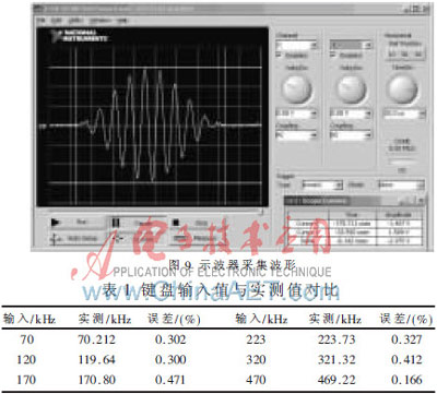
5 Experimental Results Analysis After the system is powered on, select the excitation frequency value on the keyboard as 70 kHz. Use the virtual oscilloscope of NIPCI-5102 digitizer to collect and analyze the output signal. The captured signal is shown in Figure 9. It can be seen from the panel parameters that the maximum amplitude of the waveform is 1.5V, and the narrow-band pulse width of a single-tone signal including 10 cycles is about 0.142ms. Change the keyboard input and perform FFT spectrum analysis on the output signal, as shown in Table 1. Experimental results show that the excitation signal generated by this design has high accuracy, pure waveform, good performance, and continuously adjustable frequency, which satisfies the design requirements.
Using SoPC technology, a new design method of ultrasonic guided wave excitation signal generator is given. Focuses on the implementation process of waveguide-specific DDS modules. Integrate the main functions of the system into a single FPGA, reducing the peripheral circuit, small size, low power consumption, strong anti-interference ability, easy to expand and upgrade, and effectively reduce the design cost. The resulting excitation signal has high accuracy, good stability, and continuously adjustable frequency. This design can be easily applied to the detection of ultrasonic flaws in pipelines, and offers the possibility to develop a miniaturized and integrated guided wave detection system.
References[1] Wu Bin,Deng Fei,He Cunfu.Research progress in signal processing in ultrasonic guided wave nondestructive testing[J].Journal of Beijing Polytechnic University,2007,33(4):342-348.
[2]Wang Junzhen, Wang Jianbin, Wang Shuai. Design of ultrasonic guided wave excitation signal source based on DS89C430[J]. Electronic Design Engineering, 2010, 18(10): 136-138.
[3]Wu Bin, Wang Zhi, Jin Shan, et al. Arbitrary waveform generator for exciting ultrasonic guided waves [J]. Journal of Beijing Polytechnic University, 2002,28 (4): 389-393.
[4]Jin Chuanxi, Wu Xinjun, Xia Zhimin, et al. Design and application of excitation sources for guided wave detection [J]. Manufacturing Automation, 2006, 28(10): 79-81.
[5] Tian Yi, Hu Bin, Xu Wenbo, et al. XilinxISEDesignSuite10.xFPGA development guide - logic design articles [M]. Beijing: People's Posts and Telecommunications Press, 2008:27-29.
[6] Wang Jinming. Digital System Design and Verilog HDL (Third Edition) [M]. Beijing: Publishing House of Electronics Industry, 2009:285-286.
In the inspection of pipeline defects, the ultrasonic guided wave detection technology has the advantages of smaller attenuation along the propagation path and far propagation distance than the traditional non-destructive testing methods, and the characteristics of the vibration of the particles caused by the particles throughout the interior and surface of the components, thus exhibiting greater advantages[1]. ]. Ultrasonic guided wave has multi-modality and dispersion characteristics in the process of propagation. If the excitation source is not properly selected, the guided wave will be seriously dispersive, which will make the echo signal extremely complex and unfavorable for defect analysis. According to the characteristic curve of guided wave dispersion, it can be seen that in the range of 50 kHz to 500 kHz, the L(0,2) modal ultrasonic guided wave has the fastest and most stable propagation speed, and almost no frequency dispersion occurs. The Hanning window is used to modulate the single-tone signal of a certain number of cycles in this frequency band to form a narrow-band pulse as an excitation source to excite the ultrasonic guided wave dominated by the L(0,2) mode, which can minimize the dispersion. Adverse effects [2].
A variety of ultrasonic guided wave excitation signal generator designs have emerged. One is to use a multifunction function generator such as the HP33120A[3]. Due to the limited storage length of the HP33120A, interference occurs between pulses during long-distance detection, and the highest modulation frequency is not high [4]. The second is the use of single-chip control DDS chip design, high precision, but the customization is weak, and generally requires more than two DDS chips, the cost is expensive. Another method is to use a high-speed MCU to control the D/A converter chip to output the signal directly, which is convenient and easy to implement. However, the accuracy is low, the excitation frequency is limited by the MCU frequency, and it is difficult to continuously adjust. In order to solve the deficiencies of the above design scheme, this design is based on Xilinx's FPGA (Field Programmable Gate Array), using the MicroBlaze soft core processor as the control core, and using the Direct Digital Frequency Synthesizer (DDS) technology to generate a new generation. An Implementation Method of SoPC (System on Programmable Chip) for L (0,2) Modal Ultrasonic Guided Wave Excitation Source. The obtained excitation source has high precision. The number of single-tone sinusoidal waves under the Hanning window modulation is adjustable, and the frequency is continuously adjustable.
1 Overall System Design The system uses the Xilinx Spartan3E-Starter development board as the hardware platform. This development platform is rich in peripheral resources, and system design can be achieved by adding a small amount of peripheral devices. Spartan3E series FPGA is the most cost-effective FPGA chip of Xilinx, which can better meet the high integration and low cost of products [5]. Its internal MicroBlaze soft processor uses a powerful 32-bit pipelined RISC architecture that contains 32 32-bit general-purpose registers, two 32-bit special registers, and a 3/5-stage pipeline. Clock frequency up to 150MHz. Based on IBM CoreConnect technology, it provides a wealth of interface resources. The PLB (Processor Local Bus) bus provides access to the on-chip peripherals, external memory, and algorithmic blocks written based on the hardware description language. Together with other peripheral IP cores, the embedded SoPC development is completed. The SoPC implementation structure of the ultrasonic guided wave excitation source is shown in FIG. 1 .
2 ultrasonic guided wave DDSIP nuclear design 2.1 DDS algorithm principle DDS is based on the sampling theorem, through the lookup table method to generate waveforms. Usually sine wave, cosine wave, triangle wave or square wave. The complete DDS structure diagram is shown in Figure 2. Driven by the reference clock, the Nbit phase accumulator accumulates the frequency control word K, and the resulting phase code addresses the waveform memory so that it outputs the corresponding waveform amplitude value. This value is given to the DAC and low-pass filter LPF to achieve the conversion of the quantization amplitude to a smooth signal. When the phase accumulation value is greater than 2N, the phase accumulator generates an overflow and the overflow frequency is the output frequency of the DDS. The output signal frequency fout can be expressed as:
According to the principle of DDS, the number N of phase accumulators determines the accuracy of the DDS. The larger the value of N, the finer the frequency interval of the DDS is. However, as the value of N increases, the required ROM capacity will also increase exponentially. In fact, in the general system, the number of bits of the D/A converter m is fixed. Usually, the number of output bits of the accumulator is set to be N=m+2, which satisfies the requirement [6]. In the design, the DAC902 is 12 bits, the accumulator is 14 bits, and the maximum amplitude of the modulation pulse is 212, which is 4096. With Matlab, a narrow-band pulse waveform is generated that is modulated by a Hanning window for 10 cycles of a sine wave, as shown in FIG. 3 .
This design is based on DDS technology and uses VerilogHDL hardware description language to design DDS modules that directly generate guided wave excitation waveforms. The top-level principle is shown in Figure 4.
The 50kHz to 500kHz frequency of the L(0,2) modal ultrasonic guided wave refers to the frequency of the single audio signal (as shown in Fig. 3, 10 cycles, setting the tone frequency to f0) instead of the DDS output frequency fout. From Tout = 10T0, fout = f0/10. So the DDS output fout should be 5kHz ~ 50kHz. The main clock of the system is 50MHz. When the DDS output maximum frequency is 50kHz, in order to achieve a 0.3kHz (single audio 3kHz) step value, 10 cycles of narrowband pulse sampling points is not less than 100 points, in order to reduce the distortion, the clock frequency must be greater than 4.9MHz. Divide the system master clock by 10 to get 5MHz DDS clock frequency. Frequency control words take 8bit to meet the requirements.
The Accumulator module Accu accumulates the frequency control word K and sends the resulting lower 14 bits sum[13:0] to the next Reg register as a ROM address. Accu's highest bit sum[14] is a judgment bit. In the accumulation process, when the phase sum[14] is 1, the accumulator is cleared to complete one pulse emission. Then through a counter to achieve delay function, so that the excitation pulse emitted once every 1ms.
The ROM module is directly customized with ROM IP core in ISE. If more than one ROM is added to the system, and each cycle is loaded with modulation pulses of different cycles, the period of the excitation source can be adjusted. With Matlab, the narrowband pulse of Figure 3 is quantized to a 12-bit fixed-point waveform value to form a .coe file and loaded into ROM.
When the frequency control word K is set to 23, the output frequency fout is equal to 7 kHz and the corresponding single audio signal is 70 kHz. Modelsim simulation waveform shown in Figure 5.
3 System Hardware Implementation 3.1 Peripheral IP Core Mounting Using the EDK XPS, the MicroBlaze hardware platform was created. Quickly add configuration via BaseSystemBuilderWizard, such as RS232, GPIO, BRAM, etc. For self-authoring DDS modules, use the Create/ImportPeripheral tool to properly modify the two automatically generated files of userlogic and IPIF. You can attach your own logic module to the PLB bus, without too much concern for custom IP and PLB bus protocol and Interface logic. Add the own DCM clock management module in XPS to provide accurate and stable clock input for DDSIP and DAC. Finally, all peripherals are assigned addresses and port connections are established.
4 The software design software is partially written in the SDK through C language, including initialization, GPIO keyboard value reading, LCD display, DDS frequency word input and adjustment. Due to the guided wave frequency of 50kHz to 500kHz, the span is large. In order to facilitate the actual detection, the frequency coarse adjustment and the fine adjustment function are designed. The system keyboard includes Set key, Adjust key, Fine key, OK key, and Reset key. After power-on, the frequency control word K is the initial value 16. The system generates a 50kHz default frequency excitation signal. Each time you press the coarse adjustment button, the value of K increases, which corresponds to base frequencies such as 70 kHz, 120 kHz, and 170 kHz. Use Fine to fine-tune at 3 kHz steps. Write the register statement DDS_IP_mWriteReg to assign the K value to the DDS module to generate the corresponding frequency excitation signal. The program flow is shown in Figure 8.
5 Experimental Results Analysis After the system is powered on, select the excitation frequency value on the keyboard as 70 kHz. Use the virtual oscilloscope of NIPCI-5102 digitizer to collect and analyze the output signal. The captured signal is shown in Figure 9. It can be seen from the panel parameters that the maximum amplitude of the waveform is 1.5V, and the narrow-band pulse width of a single-tone signal including 10 cycles is about 0.142ms. Change the keyboard input and perform FFT spectrum analysis on the output signal, as shown in Table 1. Experimental results show that the excitation signal generated by this design has high accuracy, pure waveform, good performance, and continuously adjustable frequency, which satisfies the design requirements.
Using SoPC technology, a new design method of ultrasonic guided wave excitation signal generator is given. Focuses on the implementation process of waveguide-specific DDS modules. Integrate the main functions of the system into a single FPGA, reducing the peripheral circuit, small size, low power consumption, strong anti-interference ability, easy to expand and upgrade, and effectively reduce the design cost. The resulting excitation signal has high accuracy, good stability, and continuously adjustable frequency. This design can be easily applied to the detection of ultrasonic flaws in pipelines, and offers the possibility to develop a miniaturized and integrated guided wave detection system.
References[1] Wu Bin,Deng Fei,He Cunfu.Research progress in signal processing in ultrasonic guided wave nondestructive testing[J].Journal of Beijing Polytechnic University,2007,33(4):342-348.
[2]Wang Junzhen, Wang Jianbin, Wang Shuai. Design of ultrasonic guided wave excitation signal source based on DS89C430[J]. Electronic Design Engineering, 2010, 18(10): 136-138.
[3]Wu Bin, Wang Zhi, Jin Shan, et al. Arbitrary waveform generator for exciting ultrasonic guided waves [J]. Journal of Beijing Polytechnic University, 2002,28 (4): 389-393.
[4]Jin Chuanxi, Wu Xinjun, Xia Zhimin, et al. Design and application of excitation sources for guided wave detection [J]. Manufacturing Automation, 2006, 28(10): 79-81.
[5] Tian Yi, Hu Bin, Xu Wenbo, et al. XilinxISEDesignSuite10.xFPGA development guide - logic design articles [M]. Beijing: People's Posts and Telecommunications Press, 2008:27-29.
[6] Wang Jinming. Digital System Design and Verilog HDL (Third Edition) [M]. Beijing: Publishing House of Electronics Industry, 2009:285-286.
Outdoor Sports Products ,Sports Accessories ,Athletic Equipment ,Sports Nutrition Products
Dump Truck,Ball Valve Co., Ltd. , http://www.nbgrindingmachine.com